High-speed PCB design and compliance challenges remain central to modern electronics engineering. Baltic PCB & Systems Conference 2026 takes place on 11 December 2026 at Vilnius Tech, Faculty of Electronics. Below is a concise briefing on the technical programme, attendee mix and practical steps for commercial teams.
Dates and venue at Vilnius Tech
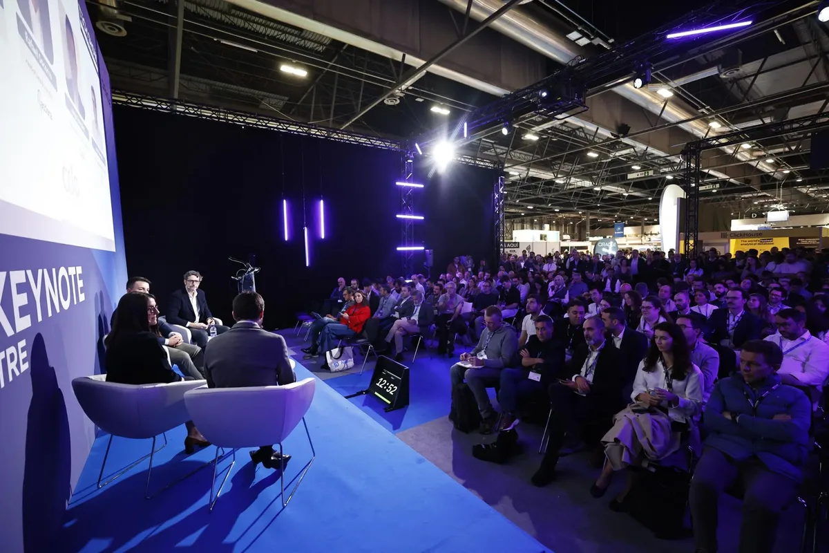
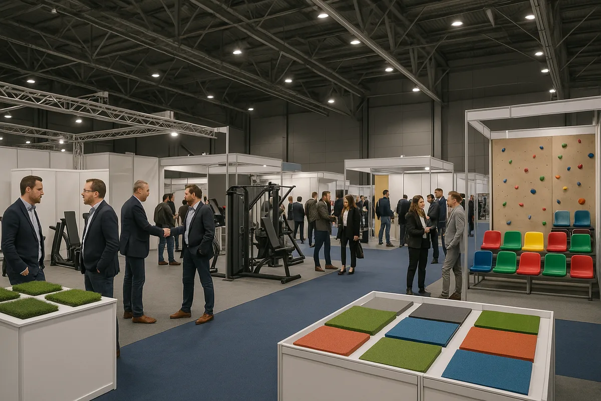
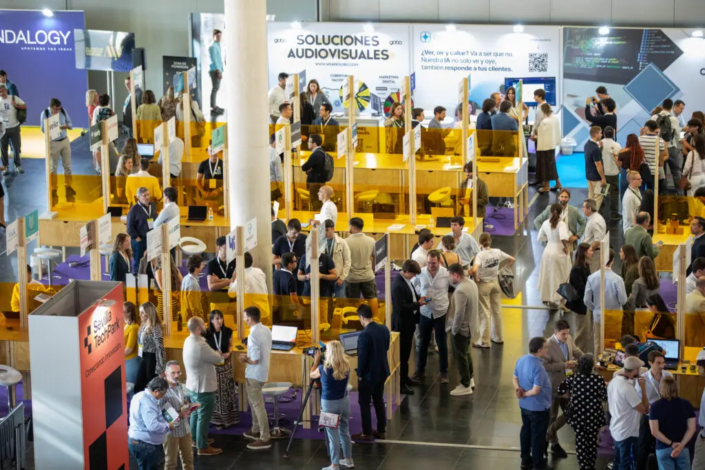
The one-day conference runs on 11 December 2026 at Vilnius Tech, Faculty of Electronics, Plytinės str. 25. Registration and morning coffee occur at Building P2, with technical sessions in Auditory 156 and the Main Hall. The venue hosts both presentations and a tech showcase area for prototypes.
Programme highlights and speakers
The agenda features two main tracks for systems reliability and design innovations. Opening remarks are delivered by Artūras Medeišis. Key sessions include shielding techniques for EMC by Piotr Gierwiatowski of Wurth Electronic and SI/PI fundamentals with André Dekker of Sintecs.
Other technical talks cover wireless device certification by Valerijus Zlosnikas of Systec Dizainas, DFT and test strategy for FPGA boards by Artur Jutman of Testonica Lab, hardware design for Cyber Resilience Act compliance by Arnas Celkys of EBV Elektronik, and a practical breakdown of PCB cost by Sergey Zorin of Dannie.CC. The programme includes coffee breaks, lunch and a networking slot where partners present demos and tools.
Attendee profile and key figures
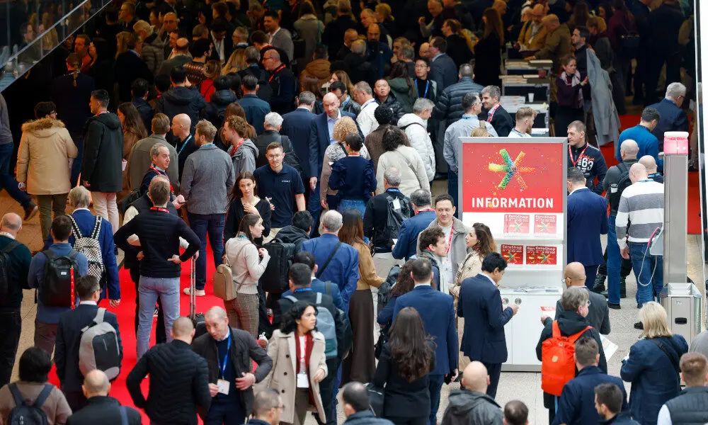
The conference gathers over 150 attendees focused on PCB design, hardware engineering and R&D management. Registered profiles include PCB designers, SI engineers, EMS engineers, HW team leads and application engineers, providing direct access to technical decision makers and manufacturing partners.
Commercial prospecting and technical positioning
Companies should approach the event with a technical sales playbook. First, map sessions that match your product capability and prepare concise technical value statements. Second, arrange short meetings with suppliers and EMS representatives to align DFM and test requirements. Third, present demos that solve explicit problems discussed in sessions such as shielding, SI/PI or test coverage for FPGAs.
Practical tips include preparing one-page technical briefs, scheduling meetings during coffee breaks and using the networking period to demonstrate quick prototypes or measurement results.
Practical information for attendees
Doors open at 9.00 with registration in Building P2. Sessions take place in Auditory 156 and the Main Hall with scheduled coffee and lunch breaks. The event also features partner promotions and a tech showcase where participants can see presented product prototypes.
Closing note and official link
For teams working on PCB design, signal integrity or hardware testability the day provides a concentrated technical exchange. Book your seat and consult the full programme on the official website http://pcbsys.eu